RF Receiver · Digital Design
Taking the amplified signal to intermediate frequency, digitising it, and getting clean complex samples to the host.
The question
Once the signal is amplified, everything that follows is a question of sampling. A commercial spectrometer hides it. Ours exposes it: we choose the intermediate frequency, the decimation, and the point at which the data becomes complex baseband.
The architecture
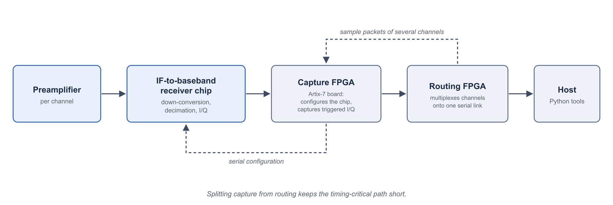
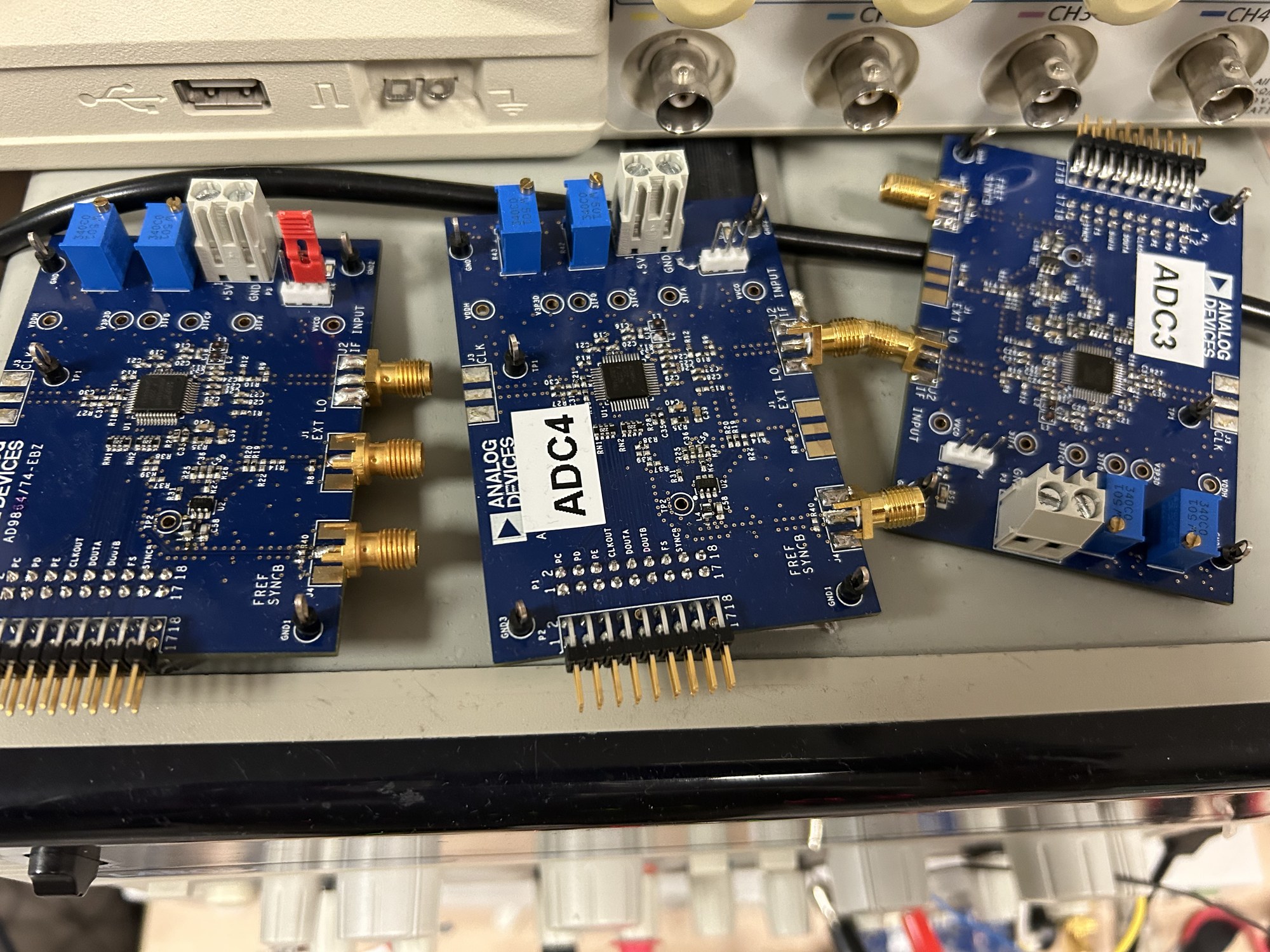
- An intermediate-frequency to baseband receiver chip performs the down-conversion and decimation, configured over a serial link from the FPGA.
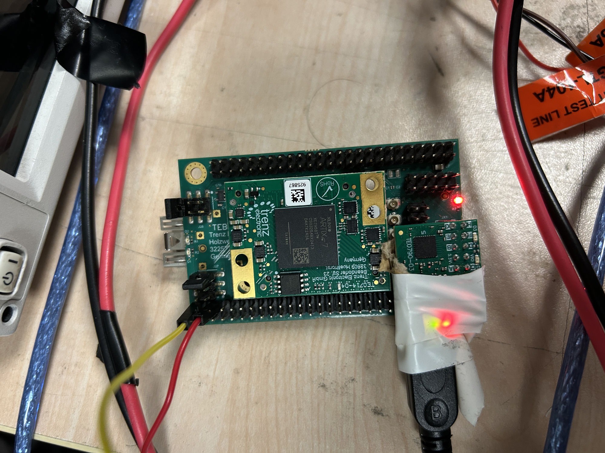
- One FPGA, on a low-cost Artix-7 development board, configures that chip and captures the triggered in-phase and quadrature sample stream.
- A second FPGA multiplexes the sample packets of several channels onto a single serial link to the host.
- Host-side tools in Python control the chain and recover the data.
Splitting capture from routing keeps the timing-critical path short.